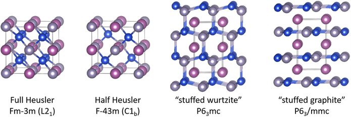
The Heusler family
We use molecular beam epitaxy (MBE) to synthesize thin films and superlattices of Heusler compounds and engineer their electronic, magnetic, thermoelectric, topological, and mechanical properties. Areas of interest include:
Epitaxy of Heusler compounds and superlattices by molecular beam epitaxy
in-situ measurements of atomic/electronic structure using scanning tunneling microscopy and photoemission spectroscopy
Properties of gapped Heuslers including thermoelectricity, topological states, half metallicity
Stabilizing new intermetallic phases including the hexagonal Half Heuslers
|
Heusler compounds are ternary variants of the cubic (zincblende) and hexagonal (wurtzite) III-V compound semiconductors.
But unlike III-Vs, they are composed of transition metals and display a diverse range of properties including both metallic and semiconducting behavior, half metallic ferromagnetism, superconductivity, heavy fermion behavior, shape memory effect, and topological behavior. |
|
bulk and nanostructured thermoelectrics
Using narrow bandgap Heusler superlattices and self assembled nanostructures
|
new Heusler variants
stabilized using epitaxial strain, for tuning topological, ferroelectric, and piezoelectric properties
|
topological materials
effects of quantum confinement, strain, and spin orbit coupling on topological candidates
|
